Welcome to Our Company

SiC BJT-MOS in R and D
Product Details:
- Usage R&D, industrial and laboratory
- Components SiC BJT, SiC MOSFET
- Features Low switching loss, fast switching, high thermal stability
- Input Standard digital/analog signal
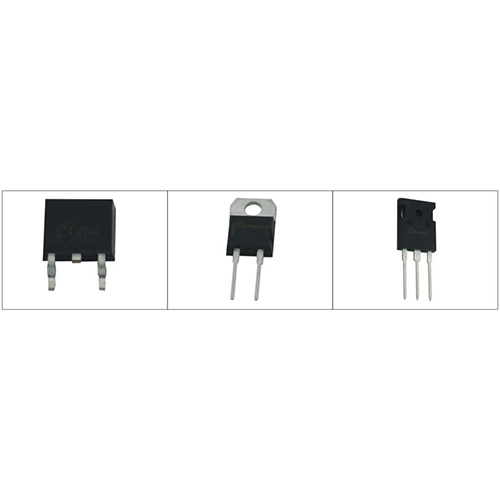
- Interface Solder pin/PCB mount
- IP Rating IP20
- Power Supply DC
- Click to view more
X
SiC BJT-MOS in R and D Product Specifications
- High current up to 50A
- High-frequency operation
- High-speed switching output
- External DC
- 600 V-1200 V
- > 3.5 W/mK
- < 25 ns
- 1200 V
- DC
- Integrated temperature sensor
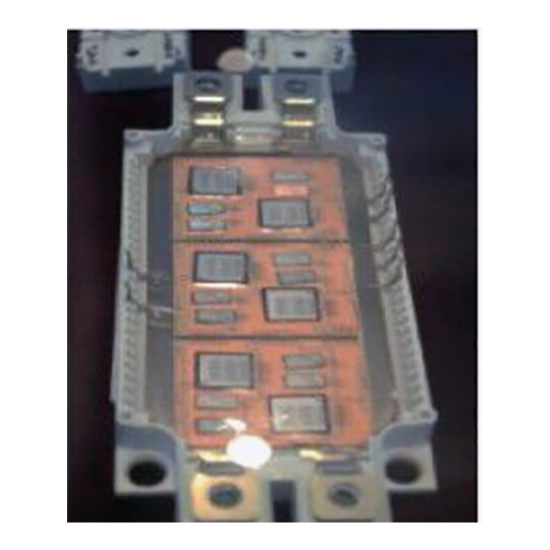
- SiC BJT-MOS hybrid module
- Up to 50 A
- -40C to 175C
- 2.5 mm
- IP20
- Power conversion, inverter, motor drives
- Standard digital/analog signal
- Solder pin/PCB mount
- Black
- 45 mm x 25 mm x 2.5 mm
- Low switching loss, fast switching, high thermal stability
- R&D, industrial and laboratory
- SiC BJT, SiC MOSFET
- Standard module size
- Approx. 50g
- Efficient power electronic switching and control
- <10 µA at rated voltage
- Yes, built-in
- Plastic molded module
- SMD or Through-hole
- Carry In
- Ultra-fast, <25 ns
- Yes
- 15 V (typical)
- 2500 V AC/min
Product Description
Silicon Carbide Bipolar Junction Transistor-Metal Oxide Semiconductor, or SiC BJT-MOS, devices are high-performance semiconductor components made for research and development purposes. With their exceptional efficiency, high voltage capabilities, and outstanding thermal stability, these devices combine the advantages of both BJT and MOSFET technologies, making them perfect for challenging situations. High-frequency applications, electric vehicles, power electronics, and renewable energy systems all frequently use SiC BJT-MOS devices. In research and development, they are essential for creating next-generation power converters, inverters, and motor control systems because of their capacity to withstand high switching rates and harsh temperatures.
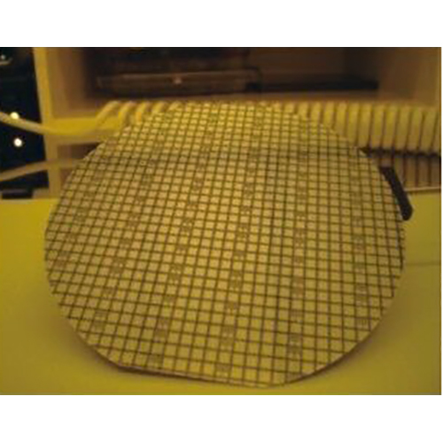
Sic BJT/MOS in R&D
Goverment project: SiC BJT: 1200V/10A SiC MOS:1200V/40m0Q/40A 1200V/80mQ/20A
Material
- High electron saturation speed (2x SD ,
- High breakdown voltage ; (10x SD ,
- Wide band gap (3x Si)
- High thermal conductivity (3x SD
- High melting point (2x SD
Devices
- Low on resistance
- High efficiency
- High voltage resistant
- High temperature resistant
Application
- Enable high speed switching rate which highly improves application efficiency
- Make equipment/ system size smaller it and lighter (such as reducing air cooling fins in PFC)
- Work steadily under high voltage environment (server in power grid)
- Work steadily under high temperature environment (EV/HEV)
|
|
|
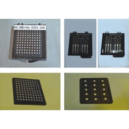
SiC diode of the company |
SiC diode of a company |
Si FRD |
Reduction rate compared with Si FRD |
|
1RM |
A |
18.1 |
16.9 |
94.8 |
80.91% |
|
Trr |
uS |
0.048 |
0.047 |
0.53 |
90.94% |
|
Qrr |
nC |
0.51 |
0.47 |
16.5 |
96.91% |
|
Erec |
mJ |
0.44 |
0.44 |
8.17 |
94.63% |
|
Eon |
mJ |
4.57 |
5.23 |
6.57 |
30.44% |
|
Eoff |
mJ |
10.23 |
10.51 |
10.27 |
0.39% |
|
Etotal |
mJ |
14.8 |
15.74 |
16.84 |
12.11% |
Ultra-Fast Switching for Advanced Applications
Designed for demanding power conversion, inverter, and motor drive systems, the SiC BJT-MOS achieves switching speeds under 25 ns, significantly increasing efficiency and response. With a 1200 V voltage rating and high-frequency compatibility, it's ideal for innovative R&D projects as well as robust industrial control.
Reliable & Safe Performance at Elevated Temperatures
Operating reliably from -40C to 175C, this module integrates ESD protection and a precise temperature sensor, ensuring consistent performance under substantial thermal and electrical stresses. Its IP20-rated enclosure and RoHS compliance make it safe for a variety of laboratory and industrial setups.
FAQ's of SiC BJT-MOS in R and D:
Q: How is the SiC BJT-MOS module used in power conversion or inverter applications?
A: The module acts as a fast-switching core in power conversion and inverter circuits, efficiently handling rapid changes in input signals to achieve reliable, high-speed switching outputs essential for modern, high-performance systems.Q: What benefits does the ultra-fast switching speed provide for R&D and industrial use?
A: With a response time of less than 25 ns, the module significantly reduces switching losses and EMI, enhancing overall system efficiency and allowing precise control in dynamic environments often required in cutting-edge research and industrial automation.Q: When should I consider using this module over traditional silicon-based switches?
A: Use this SiC BJT-MOS module when your application demands higher voltage (up to 1200V), greater thermal stability (-40C to 175C), and enhanced efficiency, particularly in high-frequency or high-current scenarios where conventional silicon devices may not perform reliably.Q: Where can the SiC BJT-MOS module be mounted or integrated within my system?
A: The module supports both SMD and through-hole mounting, allowing integration directly onto PCBs or equipment enclosures and is suitable for inclusion in power supply, inverter, and motor drive assemblies typical in laboratory and industrial projects.Q: What process is involved in interfacing the module with standard control signals?
A: The module accepts standard digital or analog control signals for the gate drive (15 V typical) and outputs high-speed switching signals. Simple solder pin or PCB mount interfaces make it straightforward to connect with existing control circuitry.Q: How does integrated ESD protection and temperature sensing enhance operational reliability?
A: Built-in ESD protection guards against static discharge damage, while the integrated temperature sensor allows real-time monitoring, ensuring the module operates within safe limits, prolonging lifespan and reducing maintenance frequency.Tell us about your requirement

Price:
Quantity
Select Unit
- 50
- 100
- 200
- 250
- 500
- 1000+
Additional detail
Mobile number
Email

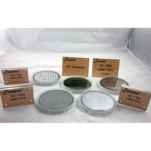
Other Products in 'SiC Device' category
Contact Details
- Rome 2401, Block B, Times Apartment, Anshanxi Street, Nankai Dist., Tianjin - 300192, China
- Phone : 86-22-27474502
TIANJIN CENTURY ELECTRONICS CO., LTD.
- Mr. Direct Li (Sales Manager)
- Mobile : +8615222645958
- Send Inquiry

 Call Me Free
TIANJIN CENTURY ELECTRONICS CO., LTD.
All Rights Reserved.(Terms of Use)
Developed and Managed by Infocom Network Private Limited.
Developed and Managed by Infocom Network Private Limited.
 English
 Spanish
 French
 German
 Italian
 Chinese (Simplified)
 Japanese
 Korean
 Arabic
 Portuguese